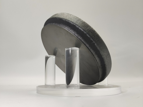
I. Core Industrial‑Application Value and Machining Bottlenecks of Silicon Carbide Substrates
Amid the rapid iterative development of third‑generation semiconductors, silicon carbide (SiC) outperforms silicon‑based and gallium‑arsenide materials in physical and chemical properties. It has become a core substrate material for high‑voltage power semiconductors, radio‑frequency devices, and new‑energy power‑electronic equipment. Featuring an ultra‑wide bandgap, superior thermal conductivity, high breakdown electric‑field strength, fast electron saturation velocity, as well as outstanding radiation resistance and high‑temperature tolerance, SiC perfectly fits demanding operating scenarios such as new‑energy‑vehicle electronic control systems, photovoltaic and wind‑power inverters, high‑voltage charging piles, and high‑power aerospace devices. It represents a foundational material for the ongoing upgrading of the semiconductor industry.
Nevertheless, the intrinsic material properties of SiC crystals constitute major bottlenecks restricting large‑scale mass production and yield improvement. On one hand, silicon carbide is an ultra‑hard‑to‑machine material with a Mohs hardness of up to 9.5, close to that of diamond. On the other hand, it exhibits extreme chemical inertness and barely reacts with acid or alkaline reagents under ambient and conventional‑process conditions. These two characteristics make it difficult for traditional wafer‑processing technologies to simultaneously satisfy three key requirements: machining efficiency, surface flatness, and freedom from subsurface damage. This significantly raises the manufacturing cost of
SiC substrates and hinders the widespread adoption of third‑generation‑semiconductor devices.
II. Inherent Drawbacks of Conventional SiC‑Substrate Machining Processes
The mainstream industrial workflow for SiC‑substrate fabrication is: crystal growth → orientation‑dependent slicing → edge rounding and lapping → wafer thinning → precision polishing. Slicing, thinning and polishing are critical steps that define the final substrate quality and are also the primary sources of processing‑induced defects. Currently commercialized polishing techniques are all contact‑type processes, including mechanical polishing, chemical‑mechanical polishing (CMP), electrochemical‑mechanical polishing (ECMP), and magnetorheological finishing (MRF).
A fundamental disadvantage of such processes lies in direct mechanical contact between abrasives/fixtures and the wafer surface. Extrusion and shear stress are applied during processing, readily introducing microcracks, lattice dislocations, residual stress, scratches and other defects in the near‑surface and subsurface layers. The electrical performance, stability and service life of semiconductor devices are highly dependent on substrate surface quality and lattice integrity. Even minor subsurface damage can trigger defects in subsequent epitaxial growth, device current leakage, and degradation of voltage‑withstanding capability.
To eliminate machining‑induced damage, manufacturers must implement additional rounds of fine polishing and cleaning. These steps extend production cycles, lower throughput, and substantially increase consumable and labor costs. This explains the current shortage and high price of high‑end SiC substrates. Therefore, the industry urgently demands a novel non‑contact machining technology that delivers zero mechanical damage, high throughput and precise surface modification to break through the limitations of conventional processes.
III. Atmospheric‑Pressure Plasma Etching: A New Route for Damage‑Free SiC Machining
Atmospheric‑pressure plasma etching is a multi‑physics‑field‑coupled dry‑chemical machining technology. Unlike traditional physical grinding, it involves zero mechanical contact and zero applied stress, fundamentally eliminating surface and subsurface damage to SiC wafers. It serves as a promising process for ultra‑precision modification of high‑end SiC substrates. Operable at room temperature and atmospheric pressure without vacuum hardware, it offers advantages of low cost, high efficiency and easy industrialization.
Its core mechanism relies on fluorine‑based chemical etching reactions, proceeding in three consecutive closed‑loop stages:
1.
Plasma excitation: Argon (Ar) is fed as a carrier gas into the plasma torch. Ionization occurs under a high‑frequency RF power supply to generate a stable plasma jet. High‑energy electron collisions dissociate carbon tetrafluoride (CF₄), producing abundant reactive fluorine atoms and fluorine radicals (F*).
2.
Surface chemical reaction: Highly reactive F* species adsorb onto the
SiC wafer surface and selectively react with silicon components in the material.
3.
Volatile by‑product removal: Gaseous silicon tetrafluoride (SiF₄) is generated as the reaction product and rapidly carried away from the wafer surface by the plasma jet, yielding a flat, damage‑free substrate surface.
Core reaction formula:
SiC+F∗→SiF4↑
IV. Experimental Setup and Inspection System (with annotated figures)
The atmospheric‑pressure plasma machining system built in this study consists of five modules: plasma generator, three‑axis motion‑control unit, high‑precision gas‑supply unit, temperature‑measurement unit and topography‑inspection unit. It enables localized, site‑specific modification of SiC wafers.
 Figure 1: Diagram of plasma‑torch machining process
 The plasma generator is the core unit, composed of a 40.68 MHz high‑frequency RF power supply, impedance matcher, plasma torch tube, induction coil and spark igniter. Its power is adjustable within 5–1000 W, and forced air‑cooling ensures stable equipment operation. The three‑axis motion stage has travel of 600 mm × 600 mm × 400 mm, with bidirectional positioning accuracy of 10 μm and repeat positioning accuracy of 5 μm to guarantee precise machining placement.
 Figure 2: Schematic diagram of thermal‑imaging pyrometer measurement
 A thermal‑imaging pyrometer is mounted orthogonally to the plasma jet for real‑time monitoring of torch temperature and overall jet temperature‑field distribution, preventing wafer damage caused by thermal effects. Post‑processing inspection employs a Taylor Hobson PG1830 roughness profilometer for high‑precision characterization of machined‑site topography, etch depth and surface roughness.
V. Key Evaluation Metrics for SiC Plasma Machining
Experimental characterization demonstrates that the material‑removal profile created by the plasma jet on
SiC wafers presents a rotationally symmetric Gaussian surface with excellent fitting quality. The machining effect can be accurately quantified by Gaussian functions. Three primary evaluation indicators are defined:
1.
Peak removal rate (a): The maximum etch depth per unit time on the wafer surface, directly representing instantaneous material‑removal capacity.
2.
Full width at half maximum (FWHM): Lateral machining width measured at half of the peak removal depth, denoting the effective processing range of the plasma.
3.
Volumetric removal rate (V): Total volume of SiC removed per unit time, a key metric for process throughput and mass‑production adaptability.
 Figure 3: Machined point material removal contour
 Figure 4: Removal function configuration bus diagram
 Figure 5: Comparison between removal contour and Gaussian fitting curve
 In summary, atmospheric‑pressure plasma etching abandons the physical‑grinding paradigm of conventional contact‑type machining and addresses major industry pain points for SiC substrates: difficult‑to‑cut ultra‑hard nature, contact‑induced damage, and excessive polishing costs. Nevertheless, process performance is highly sensitive to parameters such as gas‑mixture ratio, machining power, and torch‑to‑target distance. A follow‑up article will provide an in‑depth analysis of parameter‑dependent effects from three key process gases and practical engineering mitigation strategies.
Jingmu Optoelectronics supplies full‑spec silicon carbide substrates, covering 2‑ to 12‑inch standard wafers as well as small‑size square coupons. Conductive, semi‑insulating and special‑crystal‑type variants are available. Customization of thickness, crystal orientation and dimensions is supported for R&D, pilot‑scale testing and full‑scale mass‑production scenarios.